

Top 10 Quartz Crucible Options for High-Purity Material Processing
2026-11-02
Choosing the right quartz crucible can make or break your high-purity material processing run. Contamination, thermal shock, and dimensional drift aren't just annoyances—they're yield killers. In this roundup, we cut through the noise to highlight ten crucible options that actually hold up under demanding conditions. Whether you're pulling silicon ingots or refining specialty alloys, the details matter. And if you've been burned by inconsistent suppliers, you'll appreciate how Semicorex approaches quality control with a level of rigor that rarely shows up in spec sheets. Read on for the shortlist that could save your next batch.
When the Crucible Walls Start Writing Your Contamination Report
The crucible sat cooling on the bench, its ceramic surface still warm from the last firing. Under the overhead lamp, the inner walls caught the light oddly — not with the usual dull gray of spent ash, but with a faint, almost organic mottling. Someone had scrawled a message there, not in ink but in residue. A streak of rust near the rim. A bloom of white crystals clustered at the base. It looked less like contamination and more like a report written in a language only the furnace could read.
Each mark on the wall had a specific origin. The rust streak traced back to a steel spatula used once for a sulfate fusion, then rinsed too briefly. The crystal bloom formed where leftover borate flux had wicked up the side during a slow cool-down, dragging impurities with it. A faint blue-gray haze near the lip signaled volatilized copper from a previous assay, never fully removed by the last acid wash. None of these came with labels, but the pattern matched a log of shortcuts and oversights that no one had bothered to write down.
After a while, you stop seeing the crucible as a passive container. It becomes an archive of every mistake made in its presence — the rushed cleaning, the wrong temperature ramp, the reused lid from a different project. Most contamination reports get filed away on clipboards or buried in spreadsheets. But the most accurate one was already written, layer by layer, on the inside of a piece of fired clay. The trick is learning to read it before the next run turns those marks into bad data.
Fused vs. Sintered: The Split That Shows Up in Your Yield
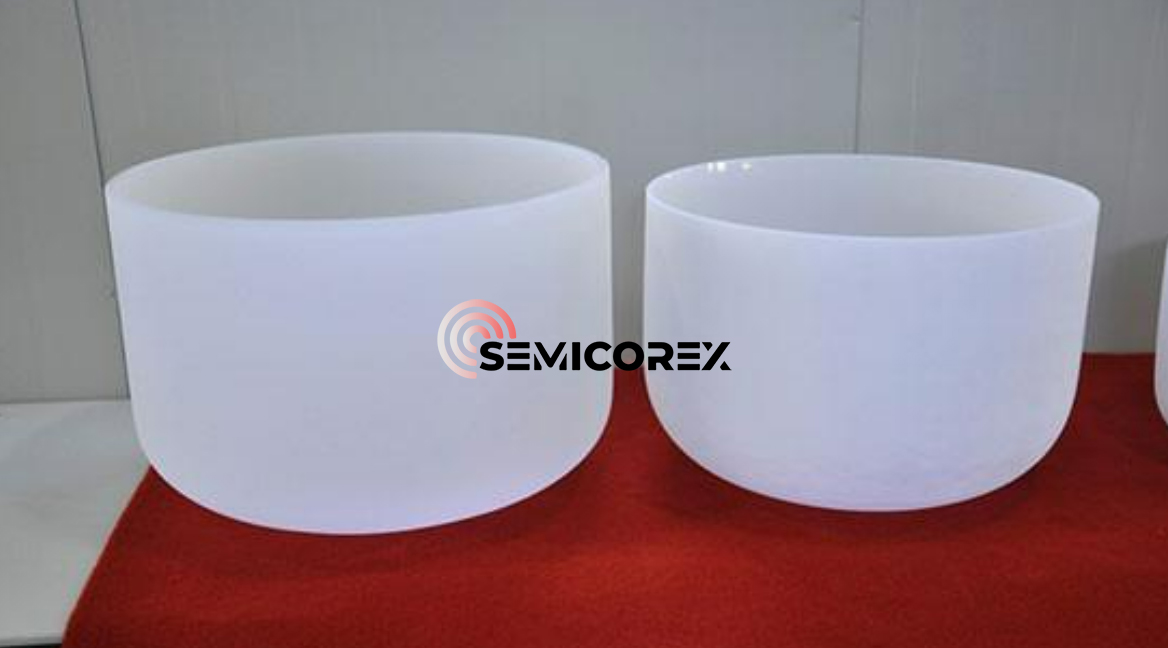
The moment you see a yield drop that no amount of process tweaking seems to fix, the culprit is often hiding in the material itself. Fused and sintered components can look nearly identical on a spec sheet, but their internal structure tells a completely different story. Fused parts tend to have fewer internal boundaries and a more uniform density, which translates to consistent thermal and electrical behavior across the batch. Sintered parts, on the other hand, carry the fingerprint of their powder origins—microscopic voids, irregular grain growth, and localized density variations that quietly eat away at performance when you push the device to its limits.
Where this really bites is in high-frequency or high-temperature applications. A fused element gives you a predictable response from one unit to the next, because the material acts as a single continuous medium. A sintered element, even from the same nominal composition, can scatter your yield data with subtle variations in impedance, thermal conductivity, or mechanical stress tolerance. One batch might pass final test with flying colors, while the next batch—same furnace profile, same operator—shows a 3% fallout that nobody can explain until they cut a cross-section and see the porosity.
So before you rewrite the entire process flow, take a hard look at what the material is doing. If you're chasing a yield gap that moves around from lot to lot, the difference between fused and sintered is often the lever you haven't pulled. Swapping to a fused version of the same part isn't always cheap, and it's not always necessary—but when your end-of-line numbers keep slipping through your fingers, that structural split is usually where the loss is hiding.
Why Vacuum Baking Shifts the Trace Metal Conversation
Vacuum baking doesn't just remove moisture—it rearranges the entire debate around trace metals. Under normal atmospheric heating, surface oxides and adsorbed contaminants linger, often masking the true metal content or shifting oxidation states in ways that skew analytical results. By pulling a vacuum first, you strip away the volatile layers that typically dominate the conversation, forcing a sharper focus on the metals that actually matter for performance or safety.
The shift happens because vacuum baking creates a cleaner baseline. Trace metals that were previously hidden inside hydrated films or bound to organic residues become detectable without the noise of thermal decomposition byproducts. This changes what we call “trace” in the first place—levels that once seemed negligible now stand out clearly, and contamination sources get re-evaluated. Instead of chasing after bulk contamination, engineers and chemists start talking about surface-bound species that only emerge once the usual hiding spots are gone.
In practice, this means old assumptions about metal leaching, catalytic poisoning, or even biocompatibility need a second look. A part that tested clean after conventional drying might reveal unexpected chromium or nickel after vacuum baking, simply because the background was quieter. The conversation moves from “how much metal is present” to “what form is it in, and where did it come from,” which is a far more useful question when trace metals are the difference between a reliable component and a field failure.
Matching Thermal Expansion to Your Real Heating Curve
A real heating curve rarely behaves like the neat, linear ramp printed in a manual. Your kiln, furnace, or process line may lag behind the setpoint, overshoot during transitions, or hold unevenly across the load. Matching thermal expansion to that actual curve means tracking the temperature where your material really sits, not where the controller claims it should be. A thermocouple placed near the work, logged over several cycles, will show subtle plateaus and surges that published expansion data simply cannot anticipate.
Look for the moments when expansion rate shifts abruptly, often tied to moisture release, binder burnout, or a phase transformation. Those are the places where stress builds if the outer surface moves faster than the core. Instead of forcing a fixed ramp, adjust the hold time or reduce the heating rate just before each inflection point. Even a ten-minute soak at 200°C or a slower climb through quartz inversion can bring the expansion behavior of the piece in line with the heat actually delivered.
A practical method is to overlay a dilatometry curve onto your logged heating data. Where the two lines diverge, you have a mismatch zone. Insert a brief dwell or soften the ramp there, then run a test piece and check for micro-cracks or warpage. Over a few firings, the adjustments become almost intuitive, and the result is fewer failures without chasing an idealized profile that never existed in your equipment.
Surface Roughness: The Quiet Variable in High-Purity Melts
Ask a process engineer about the variables that matter in high-purity melt handling and you'll likely hear about oxygen levels, thermal gradients, and container material. Surface roughness seldom makes the list. That's a blind spot. The texture of the crucible or mold wall, down to the sub-micron scale, governs how the melt wets the surface, where the first solids form, and how much of the container ends up in the final product.
Most contamination in high-purity melts doesn't come from bulk dissolution; it comes from microscopic high points where the melt attacks the container more aggressively. A rough surface also creates local flow disturbances that hold impurities near the wall instead of letting them be swept away. In silicon crystal growth or superalloy remelting, these subtle effects show up as unexplained inclusions, off-spec resistivity, or poor single-crystal yield.
Fixing the problem isn't as simple as ordering a finer polish. Depending on the melt chemistry and solidification mode, some surfaces need controlled roughness to prevent cracking or gas entrapment, while others need near-perfect smoothness. The only reliable approach is to measure roughness with the same rigor as temperature and treat it as a specification, not an afterthought. Teams that do this usually find that the "quiet" variable was louder than they expected.
What Suppliers Won’t Say About Their Quartz Source
Quartz suppliers love to talk about colors and finishes, but they rarely volunteer where the raw stone actually comes from. A slab labeled as “premium” may have been cut from a block that mixed material from two or three different quarries, sometimes on different continents. That blending isn’t necessarily a problem for performance, but it does mean the batch you saw in the showroom isn’t the exact mineral composition you’ll get in your kitchen. Color consistency, resin content, and even the way the surface takes a polish can shift from one shipment to the next, and most suppliers would rather not call attention to that.
Another quiet issue is traceability. Many brands rely on a chain of brokers and processors, so by the time the slab reaches a fabricator, the mine-of-origin paperwork can be thin or entirely absent. If you ask directly, you might hear a vague answer about “multiple trusted sources” or “proprietary blends.” That’s often code for “we don’t actually know where every part came from.” The best suppliers can show you a mill certificate or at least name the region and the processing facility; the rest just hope you won’t ask.
FAQ
Purity of the raw quartz matters most, followed by dimensional stability under thermal stress. Look for low hydroxyl content and minimal metallic impurities like iron or aluminum, since these leach into melts and ruin semiconductor yields. Wall thickness uniformity also prevents cracking during rapid heating.
Arc-fused quartz typically contains fewer bubbles and has better resistance to devitrification at prolonged high temperatures, so crucibles last longer in continuous operations. Flame-fused material is cheaper but may form cristobalite spots sooner, leading to microcracks after repeated cycles.
Czochralski silicon crystal pulling and gallium arsenide synthesis require virtually flawless crucibles because any surface imperfection or trace contaminant disrupts single-crystal growth. Specialty glass melting for optical fibers also uses premium grades, though tolerance there is slightly more forgiving.
Reuse is possible only if you remove all residual material before it solidifies and etches the inner surface. A dilute hydrofluoric acid rinse followed by high-purity water works, but repeated exposure to alkali metal vapors will eventually cloud the wall and promote devitrification.
Bubbles trapped in the crucible wall act as nucleation sites for premature crystallization and can trap contaminants. For high-purity work, opt for low-bubble or bubble-free grades, even if they cost more, because they reduce particle shedding into the melt.
Keep ramp rates below 5°C per minute through the alpha-to-beta quartz transition around 573°C. Faster heating creates thermal gradients that cause microcracks, especially in large-diameter crucibles. After the transition, you can increase rates but avoid shocks above 1100°C.
Platinum and iridium crucibles outperform quartz for extreme purity in small-scale laboratory work, but their cost and softness at high temperature limit industrial use. Silicon carbide and alumina offer better thermal shock resistance but introduce more impurities, so quartz remains the pragmatic choice for most semiconductor and photovoltaic steps.
Conclusion
When contamination appears in a high-purity melt, the first place to inspect is often the crucible wall, not the feedstock. Sintered quartz looks cheaper, but its porous body creates extra surface area for grain-boundary diffusion and trapped residues, which fused quartz largely avoids. Even so, not all fused crucibles behave the same: the real differentiator is the raw quartz source, a detail suppliers rarely volunteer without pressure. Vacuum baking shifts the trace metal conversation because it strips away loosely bound alkali and transition metals before the first heating cycle. A pre-baked crucible can cut background contamination enough to matter in semiconductor or photovoltaic crystal growth, yet many buyers skip this step because suppliers treat it as an optional upgrade rather than a standard process. Matching thermal expansion to the actual heating curve is another overlooked point. If the crucible expands faster than the furnace profile, micro-cracks form at grain boundaries, releasing particles later. These cracks are invisible after cooling, but they show up as yield hits downstream.
Surface roughness is a quiet variable: a smooth inner wall gives fewer nucleation sites for unwanted crystal formation and less area for metals to leach. A rough, machined surface can undo the gains from a high-purity fused body. Suppliers often avoid discussing quartz source in detail, but the difference between synthetic quartz and naturally mined high-purity pebble is measurable in background iron and aluminum. When comparing the ten quartz crucible options for high-purity material processing, treat vague datasheets as a warning. Ask for lot-specific ICP-MS results before and after vacuum baking, plus thermal expansion coefficients and surface roughness values. The most reliable choices come from makers who are willing to release that data alongside the crucible, because those are the ones who understand that high-purity processing is a system, not just a part number.
Contact Us
Contact Person: Svenja Wei
Email: [email protected]
Tel/WhatsApp: +8613567891907
Website: https://www.semicorex.com